- 您现在的位置:买卖IC网 > Sheet目录1246 > SY87701LHI-EVAL (Micrel Inc)BOARD EVAL SY87701 EXPERIMENT
�� �
�
�SY87700/701�
�Micrel�
�FUNCTIONAL� DESCRIPTION�
�The� evaluation� board� simplifies� test� and� measurement� of�
�the� SY87700� and� SY87701.� This� section� covers� the� various�
�parts� of� the� SY87700/701� evaluation� board,� and� includes�
�detailed� information� about� these� blocks.� Performance� of�
�the� SY87700/701� can� be� easily� evaluated� by� following� the�
�step-by-step� instructions� found� in� the� “Test� Configuration”�
�section.�
�Power� Supply�
�The� SY87700L� and� SY87701L� are� 3.3V� devices.�
�Therefore,� V� CC� should� all� be� connected� to� 2.0V,� and� GND�
�connected� to� 0V,� and� V� EE� should� be� connected� to� –1.3V.�
�The� SY87700V� and� SY87701V� are� 5.0V� devices,� therefore,�
�V� CC� should� be� connected� to� 2V,� and� GND� to� 0V,� and� V� EE�
�should� be� connected� to� –3V.�
�Board� Design� and� Layout�
�The� evaluation� board� uses� a� force-sense� design� on� the�
�signal� inputs� where� the� signal� pins� (source� pins)� on� the�
�SY87700/701� are� located� on� 50� ?� line,� on� the� last� layer.�
�The� sense� lines,� however,� are� located� on� layer� 1.� The� force-�
�sense� design� is� handy� for� monitoring� inputs� to� the� SY87700/�
�701� (such� as� input� jitter).� However,� a� 50� ?� terminator� needs�
�to� be� added� to� all� unused� sense� outputs� or� the� line� will� act�
�as� a� quarter� wave� stub� notch� filter.�
�LED�
�The� SY87700/701� evaluation� board� features� one� LED�
�for� monitoring� the� Link� Fault� Indicator� (LFIN)� pin.� The� LED�
�will� turn� on� when� the� PLL� has� locked-on� to� the� RDIN� input�
�data� stream,� which� indicates� that� LFIN� has� gone� active�
�HIGH.� Additionally,� LFIN� can� only� go� active� when� CD� is�
�HIGH� and� RDIN� is� within� the� 1000ppm� frequency� range� of�
�the� PLL.�
�Signal� Inputs�
�Signal� RDIN� is� 3.3V/5V� PECL� DC-coupled.� Therefore,�
�the� current� level� for� DC-coupled� applications� is� V� CC� –2V.�
�RDIN-DRIVEN�
�Evaluation� Board�
�RDIN-BERT�
�If� you� are� using� a� high� frequency� bit� error� rate� tester�
�(such� as� the� Agilent� 70843B� Error� Performance� Analyzer)�
�to� drive� RDIN� ±� ,� you� will� need� to� insert� a� 250ps� Transition�
�Time� Converter� (TTC)� to� slow� its� edge� down.�
�REFCLK�
�If� you� are� using� a� high� frequency� clock� or� pulse� generator�
�such� as� the� Agilent� 8133� to� drive� REFCLK,� you� will� need� to�
�insert� a� 2000ps� Transition� Time� Converter� (TTC)� to� slow� its�
�edge� down.�
�Signal� Outputs�
�The� SY87700/701� features� PECL� outputs� for� both�
�RDOUT� ±� and� RCLK� ±� and� TCLK� ±� .� Unused� pins� should� be�
�left� FLOATING.�
�Test� Configuration�
�This� section� contains� step-by-step� instructions� for�
�configuring� the� SY87700� and� SY87701� for� clock� and� data�
�from� the� data� stream� of� a� BERT� stack.�
�1.� Set� switches� on� evaluation� board� for� desired� data� and�
�clock� frequencies.� There� are� seven� switches� in� SW1:�
�1.� FREQSEL1�
�2.� FREQSEL2�
�3.� FREQSEL3�
�4.� CLKSEL�
�5.� DIVSEL2�
�6.� DIVSEL1�
�7.� CD�
�See� “� All� Possible� Legal� Frequency� and� Divide� Selec-�
�tions� ”� section� on� page� 5,� on� how� to� set� these� switches.� In�
�addition,� CLKSEL� should� be� set� HIGH� which� configures�
�TCLK� output� as� the� recovered� CLK� from� RDIN.� If� CLKSEL�
�is� low,� TCLK� will� be� the� synthesized� clock� output.� Addition-�
�ally,� CD� should� be� set� HIGH� to� allow� the� PLL� to� recover�
�RDIN.� If� CD� is� low,� RDIN� is� forced� low.�
�V� CC�
�V� CC�
�2.� Connect� GND� to� 0V.�
�3.� Connect� VCC� to� +2V.�
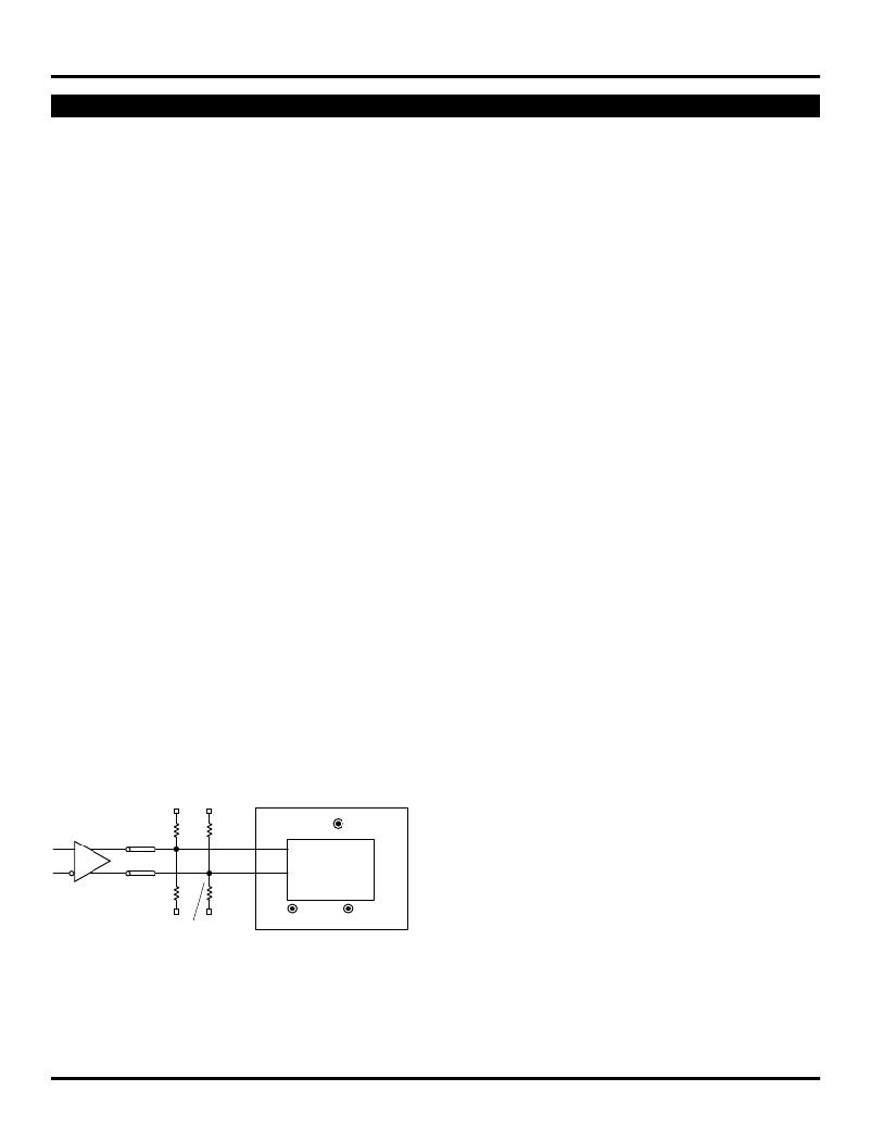
�Z=50� ?�
�Z=50� ?�
�R1�
�R2�
�R1�
�R2�
�J4�
�J5�
�RDIN+�
�RDIN� –�
�GND� 0V�
�V� CC� +2V�
�V� EE�
�4.� For� 3.3V� operation,� connect� VEE� =� –� 1.3V.�
�For� 5.0V� operation,� connect� VEE� =� –� 3.0V.�
�5.� Connect� REFCLK� (TTL)� inputs� to� reference� clock.�
�Note:� If� using� Agilent� 8133A� Pulse� Generator,� use�
�250ps� Time� Transistion� Converters� on� the� 8133�
�Note:� For� +5V� systems�
�R1� =� 82� ?� ,� R2� =� 130� ?�
�For� +3V� systems�
�R1� =� 150� ?� ,� R2� =� 75� ?�
�V� T� =� V� CC� –� 2�
�(� –� 1.3V� for� 3.3V)�
�(� –� 3V� for� 5.0V)�
�outputs.�
�6.� Connect� TCLK� (PECL)� outputs� to� data� inputs� on� test�
�equipment.�
�7.� Connect� RDINV� (PECL)� inputs� to� data� source.�
�Figure� 2.� Test� Set-Up�
�2�
�8.� Connect� RDOUT� (PECL)� to� outputs� on� test� equipment.�
�9.� Connect� RCLK� outputs� to� clock� inputs� on� test�
�equipment.�
�发布紧急采购,3分钟左右您将得到回复。
相关PDF资料
SY87729LHI-EVAL
BOARD EVAL N SY87729 EXPERIMENT
T10C360BF
THYRISTOR TVS 360V 100A 3PIN RDL
T12-211SNR-1
CIRCUIT BRKR THERMAL 1A 1POLE
T13-212R-0.5
CIRCUIT BRKR THERMAL 500MA 1POLE
T21-A230X
SURGE ARRESTER 230V GASTUBE 3PIN
T23-A230X
SURGE ARRESTER 230V GASTUBE 3PIN
T23-A350X
SURGE ARRESTER 350V GASTUBE 3PIN
T26-2-7.00A-27720-1
CIRCUIT BREAKER 3P 7A 50V CUSTOM
相关代理商/技术参数
SY87701LHITR
制造商:MICREL 制造商全称:Micrel Semiconductor 功能描述:3.3V 32-1250Mbps AnyRate CLOCK AND DATA RECOVERY Use lower-power SY87701AL for new designs
SY87701LSI
功能描述:IC CLOCK/DATA RECOVERY 32-TQFP RoHS:否 类别:集成电路 (IC) >> 时钟/计时 - 专用 系列:AnyRate® 标准包装:1,500 系列:- 类型:时钟缓冲器/驱动器 PLL:是 主要目的:- 输入:- 输出:- 电路数:- 比率 - 输入:输出:- 差分 - 输入:输出:- 频率 - 最大:- 电源电压:3.3V 工作温度:0°C ~ 70°C 安装类型:表面贴装 封装/外壳:28-SSOP(0.209",5.30mm 宽) 供应商设备封装:28-SSOP 包装:带卷 (TR) 其它名称:93786AFT
SY87701LZG
功能描述:计时器和支持产品 3.3V Any-Rate 32-1250 Mbps CDR (I Temp, Green/28 Pin SOIC/Bulk)
RoHS:否 制造商:Micrel 类型:Standard 封装 / 箱体:SOT-23 内部定时器数量:1 电源电压-最大:18 V 电源电压-最小:2.7 V 最大功率耗散: 最大工作温度:+ 85 C 最小工作温度:- 40 C 封装:Reel
SY87701LZG TR
功能描述:计时器和支持产品 3.3V Any-Rate 32-1250 Mbps CDR (I Temp, Green/28 pin SOIC/T+R)
RoHS:否 制造商:Micrel 类型:Standard 封装 / 箱体:SOT-23 内部定时器数量:1 电源电压-最大:18 V 电源电压-最小:2.7 V 最大功率耗散: 最大工作温度:+ 85 C 最小工作温度:- 40 C 封装:Reel
SY87701LZGTR
制造商:MICREL 制造商全称:Micrel Semiconductor 功能描述:3.3V 32-1250Mbps AnyRate CLOCK AND DATA RECOVERY
SY87701LZI
功能描述:IC CLOCK/DATA RECOVERY 28-SOIC RoHS:否 类别:集成电路 (IC) >> 时钟/计时 - 专用 系列:AnyRate® 标准包装:1,500 系列:- 类型:时钟缓冲器/驱动器 PLL:是 主要目的:- 输入:- 输出:- 电路数:- 比率 - 输入:输出:- 差分 - 输入:输出:- 频率 - 最大:- 电源电压:3.3V 工作温度:0°C ~ 70°C 安装类型:表面贴装 封装/外壳:28-SSOP(0.209",5.30mm 宽) 供应商设备封装:28-SSOP 包装:带卷 (TR) 其它名称:93786AFT
SY87701LZITR
制造商:MICREL 制造商全称:Micrel Semiconductor 功能描述:3.3V 32-1250Mbps AnyRate CLOCK AND DATA RECOVERY
SY87701V
制造商:MICREL 制造商全称:Micrel Semiconductor 功能描述:5V/3.3V 32-1250Mbps AnyRate CLOCK AND DATA RECOVERY